Fixing the Bane of Costly Component Out Of Pocket Defects
August 18, 2021Mitigating the High Cost of Die Migration
by Darby Davis, Gel-Pak and Craig Blanchette, BAE Systems
Expansion in the areas of SATCOM, automotive radar, 5G, and security are pushing high frequency semiconductor technologies toward smaller thinner footprints.
These new high-performance Class III-V devices, made from materials such as GaN and GaAs, offer advanced features that enable a new generation of communication and sensing applications.
With every new advancement however, there are usually challenges to overcome. BAE Systems in collaboration with Gel-Pak did an extensive study on a significant challenge associated with the internal handling and shipping of today’s thin compound semiconductor devices.
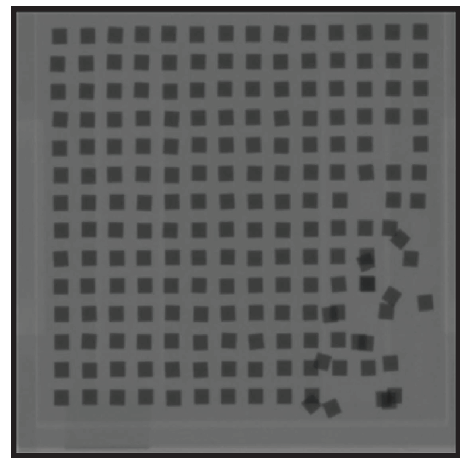
Leading semiconductor manufacturers experience issues with ultra-thin compound semiconductor die (≤250μm) migrating out of the pockets of waffle pack chip trays during shipping and handling (Figure 1). This Component Out of Pocket (COOP) condition is a significant cost driver in manufacturing operations and results in the following:
- Component damage and scrap
- Non-value added labor to inspect and re-order components
- Production interruptions
- Decreased pick and place machine utilization
- Quality Management System administration labor

Together, BAE Systems and Gel-Pak researched the root causes of this costly issue to better understand how to prevent it and save industry millions of dollars per year.
Through extensive investigation, several root causes were identified. It was found that COOP was attributed to deficiencies in the existing waffle pack tray/lid technology such as:
- Warpage common to injection molded chip trays and lids. Carbon loaded polypropylene material has an upper specification flatness tolerance of 12 mils for both the lid and the waffle pack tray, which means there is potential for a 24 mil gap from which components can migrate. ABS and carbon loaded polycarbonate material have a flatness tolerance of 4 mils for both the lid and the clip, which means there is potential for an 8 mil gap.
- Uneven stresses, caused by the industry standard one-piece clip, which deforms the chip tray and lid. A one piece clip was studied using a 3D measurement system and showed that it can impart deflections of the lid/tray due to the design, thus creating avenues for component egress. It was also discovered that when clips are re-used, springs become worn out and exert inconsistent holding force, which also contributes to COOP.
- Misalignment and/or pinching of non-woven polyethylene inserts (such as Tyvek paper) when preparing waffle pack for shipment (Figure 4). These inserts have been used for decades and their intended function is to create a softer surface for sensitive components during shipping. They are not intended to prevent die migration. These inserts are easily misaligned and can become pinched, which can create another avenue for COOP.
Working with BAE Systems, Gel-Pak engineered a patent pending Lid Clip Super System (LCS2TM) that is compatible with standard waffle pack trays. LCS2 was designed to ensure effective sealing of every pocket in order to establish a COOP-free carrier solution. The ESD Class 000 approved lid is gold in color and comprised of low outgassing, static dissipative, low density polyurethane foam and industry-approved low charging static dissipative interleaf material (either black eM-20 polystyrene or non-woven polyethylene also known as your industry standard Tyvek®).
The foam and interleaf are permanently assembled into a low charging static dissipative injection molded lid using a silicone free pressure sensitive adhesive.
The lid is combined with a highly engineered gold clip design that uniformly compresses the lid onto the tray, ensuring complete contact of the entire interleaf against the waffle pack tray surface.
The materials used for the LCS2 were selected and tested per ANSI/ESD S11.11 and provide protection for high value devices with the lowest voltage susceptibility thresholds.
To measure LCS2 lid/clip system performance, a new test method was developed using an X-ray system specifically designed count parts and to detect COOP on incoming waffle packs prior to lid removal. LCS2 performance was validated by rigorous 34” drop testing of 2mil GaN die loaded in industry standard waffle pack chip trays. X-ray imaging confirmed the absence of COOP conditions when using the LCS2.
The LCS2 was proven to solve the issue of COOP for all sized components, but especially for ultra-thin components (≤250μm). The design was engineered to tolerate warped lid and clip tray materials to ensure optimal component preservation through the effective gasketing of each and every tray pocket. LCS2 has tremendous potential to curb millions of dollars in waste and improve component process efficiencies worldwide.